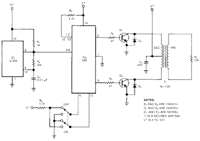
The High Voltage Inverter Circuit Diagram converts a de voltage (V +) to a high-amplitude square wave in the audio-frequency range. The dual timer, IC2, provides an inexpensive alternative to the traditional transformer for providing complementary base drive to the power transistors, Ql and Q2. You can convert a 6 to 12 V battery output, for example, to an ac amplitude, which is limited primarily by the power rating of transformer Tl.
Connect timer IC1 as an oscillator to provide a symmetrical square-wave drive to both inputs of IC2. The timing components, R2 and Cl, produce a 2.2-kHz output frequency. By connecting half of IC2 in the inverting mode and the other half in noninverting mode, the timer`s outputs alternately drive the two transistors.
Build a High Voltage Inverter Circuit Diagram
You can operate the audio-output transformer, Tl, as a step-up transformer by connecting it backwards using the output winding as an input. The transformer delivers an output voltage across RL of 4 x N x V+V pk-pk, where Nis the transformer turns ratio. For the circuit shown, the output swing is 100 x V+V pk-pk.

0 komentar:
Posting Komentar