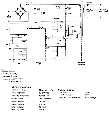
This Off line Fly back Regulator Circuit Diagram uses a low-cost feedback scheme in which the dc voltage developed from the primary-side control winding is sensed by the UC1842 error amplifier. Load regulation is therefore dependent on the j coupling between secondary and control windings, and on transformer leakage inductance.
For applications requiring better load regulation, a UC1901 Isolated Feedback Generator can be used to directly sense the output voltage.
Off line Fly back Regulator Circuit Diagram

0 komentar:
Posting Komentar