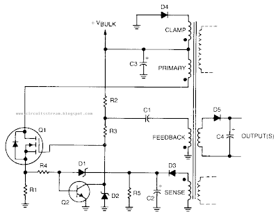
This is a Simple Self Oscillating Switching Converter Circuit Diagram. Regulation is provided by taking the rectified output of the sense winding and applying it as a bias to the base of Q2 via zener Dl. The collector of Q2 then removes drive from the gate of Ql.
Therefore, if the . output voltage should increase, Q2 removes the drive to Ql earlier, shortening the on time, and the output voltage will remain the same. De outputs are obtained by merely rectifying and filtering secondary windings, as done by D5 and C4.
Self Oscillating Switching Converter Circuit Diagram

0 komentar:
Posting Komentar