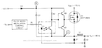
This High voltage Bucking Regulator Circuit Diagram is basically tbe classic bucking regulator, except it uses a TMOS N-channel power FET for the chopper and creates its own supply for the gate control. Tht unique aspect of this circuit is how it generates a separate supply for the gate circuit, which must be greater than Vvv.
When power is applied, C2 charges, through D2, to +12 V. At this time, Q1 is off and the voltage at point A is just below zero. When the pulse-modulated signal is applied, the optoisolator transistors, Q2 and Q3, supply a signal to Q1 that turns it on. The voltage at point A then goes to Vvn. C2 back-biases D2, and the voltage at point B becomes 12 V above Vnn· After Q1 is turned on, current starts to flow through L1 into C1, increasing until Q1 turns off.
The current still wants to flow through Ll, so the voltage at point A moves toward negative infinity, but is clamped by D1 to just below zero. Current flows less and less into C1, until Q1 turns on again. Q2 and Q3 drive Q1 `s gate between the voltages at point A and B, which is always a12 V swing, so Vcs max. is never exceeded. For proper operation, the 12-V supply has to be established before the pulse-width modulator signal is applied.

0 komentar:
Posting Komentar