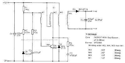
This is a Simple Portable Nicad Battery Charger Circuit Diagram. This Simple Portable Nicad Battery Charger Circuit Diagram was designed to charge NiCad battery packs in the range of 4.8 to 15.6 V from a convenient remote power source, such as an automobile batter.
When power is first applied to the circuit, a small bias current supplied by Rl via winding Wl, starts to turn on the transistor TRl. This forces a voltage across W2 and the positive feedback given by the coupling of Wl and W201uses the transistor to turn hard on, applying the full supply across W2. The base drive voltage induced across Wl makes the junction between Rl and R2 become negative with respect to the 0-V supply, forward-biasing diode Dl to provide the necessary base current to hold TRl on.
With the transistor on, a magnetizing current builds up in W2, which eventually saturates the ferrite core of transformer Tl. This results in a sudden increase on the collector current flowing through TRl, causing its collector-emitter voltage to rise, and thus reducing the voltage across W2.
The current flowing in W2 forces the collector voltage of the TRl to swing positive until restricted by transformer output loading. Rc network R4 and C3limits the turn off transient TRl. R3 and C2 maintain the loop gain of the circuit when diode Dl is not conducting.

0 komentar:
Posting Komentar