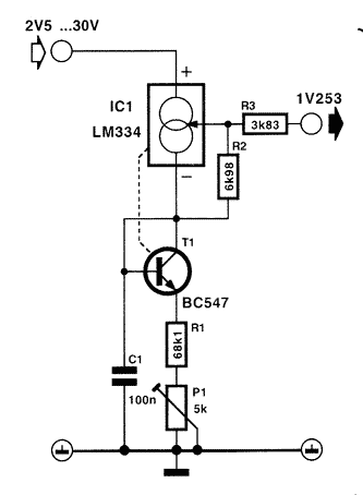
The Low Power Voltage Reference Circuit Diagram described below, is a special implementation of current source LM334. Characterized by a very small temperature coefficient metatholio output voltage and consumes only 10uA room temperature. This current fluctuates by a few uA, when the ambient temperature varies significantly. The positive rate of temperature change LM334 offset by the negative of the contact base emitter transistors has a direct thermal coupling with the integrated.
To achieve the lowest possible temperature coefficient, it is necessary to adjust the output voltage of 1,253 V source to the arrangement easily done through R1. From the moment you get the desired output voltage, you are advised to stuck P1 and after the count value, replace it with a constant resistance. The best indeed is to replace P1 with the R1, so you have fewer parts. Prefer metal film resistors and tolerance of 1% E96 series. Having as a given that the output voltage obtained from the pin configuration LM334, is expected to show a negative resistance value 3.8 KO.
The resistance A3 ensures that the output impedance will be equal to 400 W. Under these conditions, the current that can provide the source to the load to be connected to out of retained less than 5 Ma stability of the voltage source is more than satisfactory. By varying the input voltage from 5 V to 30 V, the change in output was only 0.6 mem (from 1.2530 to 1,2536 V). The change in the thermal coefficient is maintained at values ??less than 50 ppm / C, and if you worry a bit more to the setting of the circuit, you will see that quite easily reaches 5 ppm / C. The requirements of the original circuit current was only 9.8 mA at a temperature of 22C.
Low Power Voltage Reference Circuit Diagram

0 komentar:
Posting Komentar